STED principle for laser back ablation
This innovative approach combines the two known methods of Laser Induced Backside Wet Etching (LIBWE) and Stimulated Emission Depletion (STED) to realize laser based material modifications below the diffraction limit. This is especially useful for precision laser modifications of transparent materials.
Challenge
Laser based material modifications can nowadays be found in almost every aspect of modern industry. The common goal usually is to further decrease the size of the modified areas and create smaller and more precise structures. The desired domain for a lot of technical applications lies in the sub wavelength range. One way to realize this goal, is to take advantage of non-linear absorptions through short laser pulses, low wavelengths or the combination of both. However, this process is challenging to control and sensitive to fluctuations in laser intensity. LIPSS (Laser Induced Periodic Surface Structures) or methods which utilize plasmonic surface effects are alternative approaches to realize smaller laser structuring while having disadvantages like the limitation to non perfect periodic structures or the need for certain ambience conditions which limits their application.
Our solution
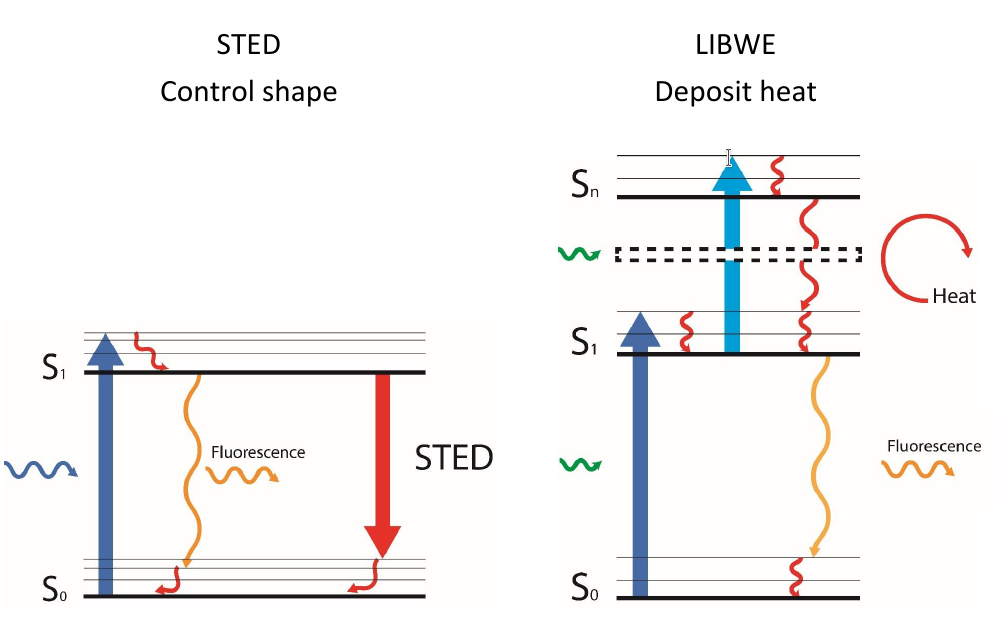
The innovative approach presented here is to combine the two methods of LIBWE and STED to realize laser based material modifications below the diffraction limit by limiting the laser energy deposition into the material spatially through optical switching between molecular states. In the default LIBWE process, a liquid that strongly absorbs the laser beam is brought into contact with the back of a transparent material. A laser passes the transparent material, hits the absorbing liquid and induces excited state absorption (ESA) in the present color molecules and therefore a large temperature and pressure difference leading to the ablation of the adjacent material. Utilizing a second laser with a donut shaped intensity profile at the same location, it is possible to relax adjacent areas around the focus spot where ESA takes place and therefore limiting the modification area or range where the ablation takes place spatially. This process leads to material modifications in the sub wavelength range.
 Schematic overview of the principle behind the combination of LIBWE with STED and the optical switching between molecular states. (source: apl. Prof. Dr. Alexander Egner, Institut für Nanophotonik Göttingen e.V.)
Advantages
- Few limitations with respect to material
- Process is easy to control
- No Restrictions regarding the achievable geometries
- No additional auxiliary objects necessary
- Structuring without (micro-)cracks
- Possibility to label plane and curved surfaces
- Integrable into existing production lines
Applications
- Marking of glass materials
- Micro optics
- Nano- and sensor technologies
- Lab-on-a-chip, micro fluids
- Medical and pharma applications
Development Status
Process successfully tested on different surfaces, proof of principle verified
Patent Status
Institut für Nanophotonik Göttingen e.V.
DE102016007736B4 (granted)
References
Contact
Dr. Maria Kamper
Patent Manager Physics & Technology
E-Mail: Diese E-Mail-Adresse ist vor Spambots geschützt! Zur Anzeige muss JavaScript eingeschaltet sein!
Tel.: +49 551 30724 159
Reference: CPA-1943-LLG
