
Z-shifter for diffractive labeling of curved surfaces
The newly developed method allows for shifting of the interference plane in the Z-direction during diffractive marking of surfaces with a grating interferometer. Plane-parallel plates are used, the rotation of which introduces a beam offset that causes a Z-shift of the interference plane when the beams are combined.
Challenge
Diffractive product markings have become firmly established in numerous branches of industry as protection against counterfeiting and as design-related markings with an elegant appearance. Such hologram-like labels can be found on banknotes, credit cards, ID documents, but also on high-quality products or packaging. In the form known to date, they are produced by molding a master stamp into soft material while the stamp is inscribed using complex lithographic techniques. These are mainly polymer films which are metallized on the back side. Product marking with holographic seals is therefore carried out by gluing on or incorporating of corresponding foils. This entails decisive disadvantages and limitations: on the one hand, in many cases it is not permissible to glue or imprint the surface to be marked. This applies in particular to high-quality sensitive workpieces in the aerospace, automotive or medical technology industries. Secondly, individualization of the holograms for each individual marking process is thus not possible.
Our solution
To solve these technological problems, the Institut für Nanophotonik Göttingen e.V. researched an alternative laser-based process that enables large-area diffractive features on arbitrary materials, especially on metals, semiconductors or highly sensitive surfaces. This process is done directly to the sample and individualized for each workpiece at a speed that is suitable for industrial use. One of the major benefits of the invention disclosed here is to realize an easily and quickly realizable Z-shift of the interference plane of the grating interferometer, without having to shift the entire interferometer, while maintaining the lateral position of the interference lines (position of the maxima and minima). Plane-parallel plates are used whose rotation introduces a beam offset that causes a Z-shift of the interference plane when both beams are recombined. This allows slightly curved objects to be labeled quickly and flexibly with diffractive structures and gives the necessary free operating space which comparable processes are lacking. An additional advantage of the method outlined here is its potential use for measuring the shape of slightly curved surfaces. With the arrangement used to date, the Z position of the workpiece surface can be positioned in the interference plane with high accuracy by observing the light reflected (or backscattered) from the material surface with a camera system that forms an image of the material surface, with the reflected (or backscattered) radiation passing through the grating interferometer and upstream scanner in the backward direction. Previously, to measure a slightly curved surface, the workpiece had to be moved in the Z direction at each lateral position to determine the respective Z coordinate.
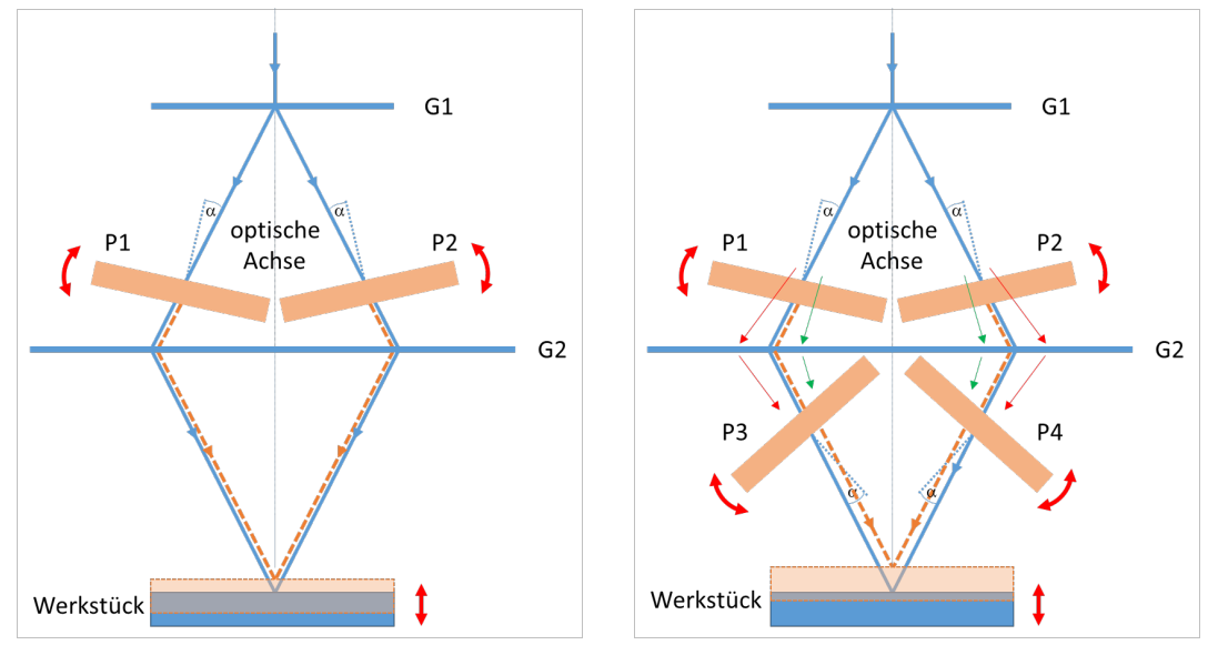 Effect of rotatable plane-parallel plates on Z-shift of the interference plane in a grating interferometer in a setup with two and four plane-parallel plates. Dotted lines illustrate the beam propagation after rotation of the plates. (source: Dr. Peter Simon, Institut für Nanophotonik Göttingen e.V.)
Advantages
- Easy Z-shift (several mm) of interference plane through rotation of two plane-parallel plates
- Allows doubling of the Z-shift by adding two additional plates
- Allows easy labeling of curved surfaces with brilliant color shine of high aesthetics
- High process speeds
- Sensitivity can be controlled by thickness of the plane-parallel plates
- Rotation of the plates by coupling with beam scanners in grating interferometer
Applications
- Design upgrade of workpieces
- Forgery-proof labeling
- Labeling of curved surfaces
Development Status
Process successfully tested on different surfaces (metal, semiconductors, plastic)
Patent Status
Institut für Nanophotonik Göttingen e.V.
DE102019133009B4 (granted)
WO2021110297A1 (disclosed)
References
Contact
Dr. Maria Kamper
Patent Manager Physics & Technology
E-Mail: Diese E-Mail-Adresse ist vor Spambots geschützt! Zur Anzeige muss JavaScript eingeschaltet sein!
Tel.: +49 551 30724 159
Reference: MM-2193-LLG